Connect with us today to learn more about our industrial automation solutions—and how to commission them for your application.
What is Reverse Engineering Pcb and Why is it Important?
Reverse Engineering Pcb is a critical process in modern electronics. It involves analyzing and recreating printed circuit boards to understand their design and functionality. Dr. Emily Johnson, a leading expert in reverse engineering, states, "Understanding the intricacies of PCB designs opens doors to innovation." Her insight highlights the importance of this field.
The process of Reverse Engineering PCB can enhance product development. Companies often use it to improve existing products. This practice helps in identifying performance gaps. In today's competitive market, staying ahead is vital. Thorough comprehension of competitor designs can foster creativity and efficiency.
However, the realm of Reverse Engineering PCB is not without challenges. Ethical implications can arise when analyzing proprietary technology. Companies must tread carefully to avoid intellectual property violations. Finding the balance between learning and respecting originality is essential. This field undoubtedly encourages innovation, but it demands responsibility and integrity.
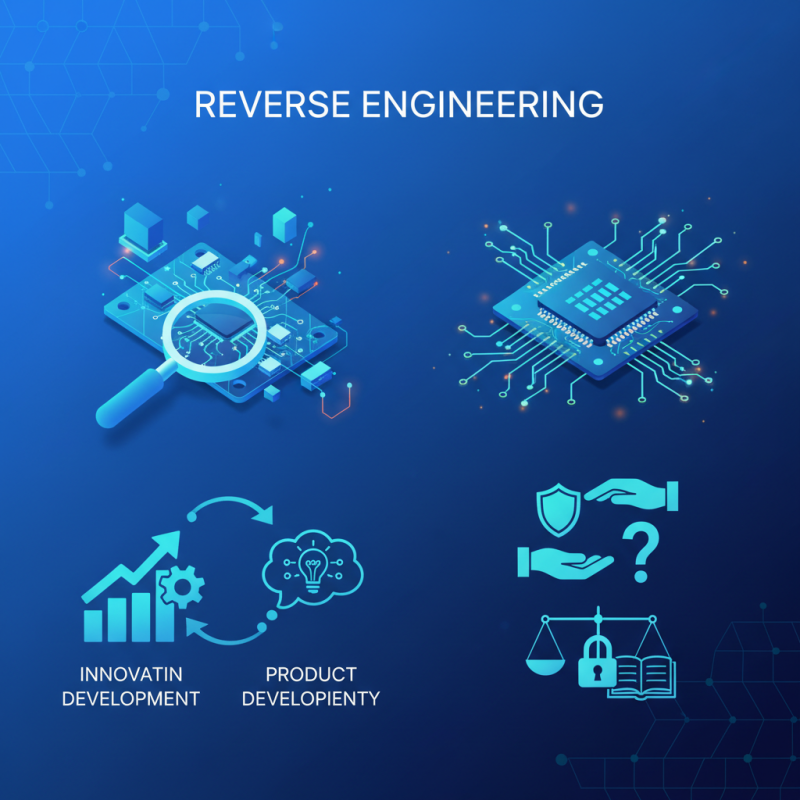
What is Reverse Engineering PCB? An Overview of the Process
Reverse engineering PCB involves breaking down a printed circuit board to understand its design and functionality. This process requires meticulous attention to detail. Engineers examine the layout, components, and connections closely. By doing this, they can recreate designs or improve existing technologies. This practice is vital in various fields, including electronics, automotive, and consumer products.
Understanding reverse engineering for PCBs can lead to innovative solutions. For example, it allows companies to identify overlooked design flaws. However, this process can be challenging. Accurate analysis requires a blend of technical skills and experience. Engineers often need advanced tools to assist in capturing complex layouts. Sometimes, there are discrepancies in the original design versus what is analyzed.
The importance of this process cannot be understated. It fosters competition and encourages advancements. It also raises ethical questions. Using reverse engineering to replicate products can lead to debates about intellectual property. Balancing innovation with respect for original designs is a nuanced challenge many face.
Reverse Engineering PCB Process Overview
This chart illustrates the time spent on each phase of the PCB reverse engineering process. Understanding the allocation of time can help optimize workflows and improve efficiency in PCB design and analysis.
The Importance of Reverse Engineering in Electronics Manufacturing
Reverse engineering printed circuit boards (PCBs) plays a crucial role in electronics manufacturing. This process involves analyzing existing designs to understand their workings. It is essential for innovation and improving product performance. Engineers and manufacturers examine a PCB to identify components, connections, and layouts. The insights gained can lead to optimized designs and reduced costs.
The importance of reverse engineering extends beyond mere understanding. It aids in diagnosing failures in existing products. When a device malfunctions, tearing down its PCB proves invaluable. Engineers can discover design flaws or suboptimal component choices. Learning from these mistakes helps prevent future issues. Furthermore, reverse engineering allows companies to stay competitive in a fast-paced market.
Industry experts often highlight the knowledge gained through this practice. However, challenges remain. Intellectual property concerns can complicate the process. Understanding ethical boundaries is vital. Not every reverse engineering attempt is straightforward. Companies must tread carefully to respect innovation while learning from it. Balancing legality and progress is an ongoing challenge in the field.
Key Techniques Used in PCB Reverse Engineering
Reverse engineering printed circuit boards (PCBs) is a fascinating field within electronics. It involves taking apart a PCB to analyze its components and design. This practice helps engineers understand the function of a circuit. It also aids in improving existing designs or creating compatible products.
Key techniques in PCB reverse engineering include schematic capture and layout extraction. Schematic capture allows engineers to identify the connections and functions of each component. This is done using software that visually represents the circuit’s layout. Layout extraction focuses on the physical arrangement of components. Engineers often use advanced imaging tools for this process, capturing high-resolution images of the PCB.
Another technique involves 3D modeling of the PCB. This helps visualize the internal structures. Sometimes, engineers face challenges with hidden or obscured elements. These small inconsistencies can lead to incorrect assumptions about the board's function. Iterative testing can refine these models, leading to better insights. Such hands-on exploration fosters innovation and deepens understanding in an ever-evolving tech landscape.
Applications of Reverse Engineering PCB in Product Development
Reverse engineering of printed circuit boards (PCBs) plays a vital role in product development. This process allows engineers to dissect existing products for purposes like understanding functionality or improving design. By analyzing a PCB, developers gain insights into component selection and arrangement. This information helps them innovate or recreate products more efficiently.
In various industries, reverse engineering is increasingly relevant. For instance, in the consumer electronics sector, companies often study rivals’ devices to enhance their offerings. In automotive and aerospace, reverse engineering aids in creating safer, more efficient systems. However, there can be challenges. Engineers must navigate the delicate balance between learning from existing designs and avoiding copyright issues.
The evolving technology landscape demands a fresh approach. As new materials and techniques emerge, traditional methods may become outdated. Yet, the fundamental goal remains: to create better products. Reflecting on past projects can illuminate areas for improvement. Understanding not only how to replicate but also to innovate can lead to groundbreaking advancements. This iterative process fosters creativity and encourages continuous evolution in product design.
What is Reverse Engineering PCB and Why is it Important? - Applications of Reverse Engineering PCB in Product Development
| Application | Description | Importance | Industry |
|---|---|---|---|
| Product Development | Analyzing existing products to design improved versions. | Helps in understanding competitors' products and achieving differentiation. | Consumer Electronics |
| Prototyping | Creating prototypes based on reverse-engineered designs. | Accelerates the product testing phase and reduces time to market. | Automotive |
| Repair & Maintenance | Identifying components for repairing non-functional PCB | Reduces costs associated with replacement and helps prolong product lifecycle. | Aerospace |
| Legacy System Support | Understanding old PCB designs to maintain outdated systems. | Ensures continued functionality and support for critical systems. | Telecommunications |
| Educational Purposes | Teaching circuit design and PCB layout techniques. | Facilitates hands-on learning and better comprehension of electronics. | Education |
Challenges and Ethical Considerations in PCB Reverse Engineering
Reverse engineering PCBs (Printed Circuit Boards) involves analyzing and reproducing the design of existing electronic circuits. While this technique has numerous applications, it comes with significant challenges and ethical considerations. For instance, the process can lead to potential intellectual property violations. Companies invest substantial resources in developing unique circuitry. Unauthorized replication can undermine their effort and innovation.
Additionally, the technical challenges of PCB reverse engineering should not be overlooked. Extracting circuit paths and understanding component interactions requires specialized expertise. Often, components are densely packed, making it difficult to trace signals. This complexity demands a deep understanding of electronics and proper tools. However, even with expertise, mistakes can occur, leading to incorrect reproductions. Such issues could cause unreliable performance or safety hazards in the final product.
Ethically, engineers must navigate a gray area. They must weigh the pursuit of knowledge against the potential harm to original creators. Transparency and respect for intellectual property rights are crucial. The engineering community must engage in open discussions about the responsible use of reverse engineering. Balancing innovation with respect for original design is a critical reflection point that professionals should regularly consider.